
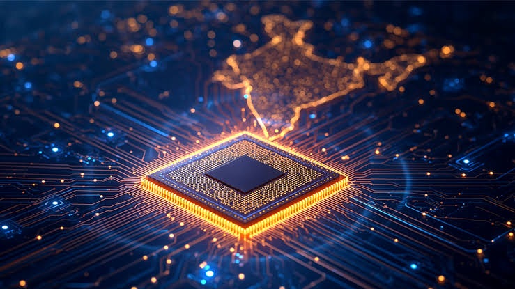
India’s semiconductor industry is moving from being largely a consumption-driven market to a broader design, manufacturing, packaging and supply-chain opportunity. Rising electronics production, electric vehicles, artificial intelligence, data centres, telecommunications, industrial automation and defence applications are increasing semiconductor demand, while government incentives are encouraging companies to establish fabrication, assembly, testing and packaging capabilities in the country.
Recent industry estimates vary depending on the definition of the market. KPMG estimates India’s semiconductor demand at around US$44 billion in 2025-26 and projects it to reach about US$90 billion by 2029-30. A UBS report estimates semiconductor end-demand could rise from US108 billion by 2030. Other industry estimates put the market at around US$100-120 billion by 2030, while the latest EY–IESA report projects the broader market could reach US$200 billion by 2035. These estimates use different market definitions and methodologies, but collectively point to strong expansion in India’s semiconductor market.
The opportunity is therefore not limited to semiconductor fabs. It extends across chip design, wafer fabrication, OSAT/ATMP, advanced packaging, semiconductor equipment, materials, chemicals, substrates, testing, cleanroom infrastructure, utilities, logistics and specialised engineering services.
The difference between India’s large demand base and its relatively small share of global manufacturing capacity points to a significant localisation opportunity. UBS estimates India currently accounts for only around 0.1% of global wafer capacity, despite representing approximately 6.5% of global semiconductor end-demand. This gap is one of the reasons semiconductor manufacturing has become a major industrial policy priority.
Sector-Wise Market Potential
According to the latest EY–IESA report, consumer electronics accounts for about 30% of India’s semiconductor market, followed by automotive at 16% and industrial applications at 15%. Together, these three segments account for more than 60% of semiconductor demand.
Consumer Electronics – 30%
Consumer electronics is currently India’s largest semiconductor demand segment. Demand comes from smartphones, laptops, tablets, televisions, wearables, smart appliances, cameras, gaming equipment, IoT devices and home automation products.
The expansion of India’s electronics manufacturing sector therefore has a direct effect on semiconductor consumption.
Government data shows that electronics production increased from approximately ₹1.9 lakh crore in 2014-15 to around ₹12 lakh crore in 2024-25. Electronics exports increased from about ₹38,000 crore to approximately ₹3.3 lakh crore during the same period.
Automotive – 16%
Automotive applications account for approximately 16% of India’s semiconductor market, according to EY–IESA.
Modern vehicles use chips for engine management, battery management, infotainment, connectivity, ADAS, sensors, power management, vehicle control systems and charging systems.
The transition towards electric vehicles is particularly important because EVs use substantial amounts of power electronics and semiconductor-based control systems. This creates opportunities for microcontrollers, power semiconductors, sensors, battery-management ICs, automotive processors and silicon-carbide devices.
Industrial Applications – 15%
Industrial applications account for approximately 15% of India’s semiconductor market. This segment includes factory automation, robotics, industrial control systems, power equipment, smart meters, renewable-energy systems, motor drives, industrial IoT, process automation and machine vision.
The expansion of India’s manufacturing sector can therefore generate semiconductor demand beyond traditional electronics.
AI and Data Centres: A New Demand Driver
Artificial intelligence is creating a new semiconductor demand cycle. AI workloads require large amounts of computing power, increasing demand for advanced processors, high-bandwidth memory, networking chips and specialised accelerators.
The relationship can be broadly represented as:
AI processors → high-bandwidth memory → networking chips → servers → storage → power systems → cooling infrastructure
India’s increasing investment in data centres therefore creates an additional demand channel for semiconductors.
Deloitte estimates India’s semiconductor market could reach approximately US$120 billion by 2030, with AI, data-centre demand, electronics manufacturing and automotive electrification among the drivers. Deloitte also estimates that India could attract around US$50 billion in semiconductor-related capital investment over the next five years.
Of this, approximately US$30-35 billion could go towards fabs and OSAT facilities, while another US$15-20 billion could be directed towards the wider value chain, including materials, gases, chemicals and equipment.
This is particularly relevant for the construction and industrial infrastructure sector because semiconductor investment generates demand well beyond the chip factory itself.
US$13 Billion Localisation Opportunity
UBS estimates India’s semiconductor market could increase from approximately US108 billion by 2030, representing roughly 15% CAGR.
More importantly, UBS estimates a US$13 billion localisation opportunity by 2030.
This indicates that India is not only expected to consume more semiconductors but could also capture a greater share of the value currently generated through imports by developing domestic manufacturing, packaging, materials, equipment and related services.
Semiconductor Imports Show the Scale of the Opportunity
India’s semiconductor imports increased from approximately US30.3 billion in FY2025, according to EY–IESA.
This represents more than a fivefold increase, with imports growing at approximately 23% CAGR over the period.
The data demonstrates the scale of India’s semiconductor consumption before large-scale domestic manufacturing has fully developed. It also explains the policy focus on domestic fabrication, OSAT, advanced packaging, semiconductor equipment, materials, chemicals, design and supply-chain development.
Major Investment Pipeline
The investment pipeline provides another measure of India’s semiconductor market potential.
As of 2026, government data indicates that 12 semiconductor manufacturing units have been approved, involving cumulative investment of more than ₹1.64 lakh crore. Three companies — Micron, Kaynes and CG Semi — have started commercial production, according to the government’s July 2026 update.
Major projects include:
Tata Semiconductor Manufacturing – Dholera
- Investment: approximately ₹91,000 crore
- Type: Semiconductor fabrication
- Capacity: around 50,000 wafer starts per month
- Location: Gujarat
Tata Semiconductor Assembly and Test – Assam
- Investment: approximately ₹27,000 crore
- Capacity: 48 million units per day
CG Power – Sanand
- Investment: approximately ₹7,600 crore
- Capacity: around 15 million units per day
Micron – Gujarat
- Investment: approximately ₹22,516 crore
- Products: DRAM and NAND assembly and testing
- Capacity: around 14 million units per week
Kaynes Semicon
- Investment: approximately ₹3,307 crore
- Focus: semiconductor packaging
Government project data also lists the Micron packaging project at around ₹13,000 crore and the proposed Tata Semiconductor Manufacturing fab at approximately ₹91,000 crore.
These projects demonstrate that the opportunity extends from fabs into packaging, testing, materials, equipment and industrial infrastructure.
Market Potential for Semiconductor Equipment and Materials
The semiconductor opportunity also extends into the upstream supply chain.
Semiconductor manufacturing requires:
- Semiconductor manufacturing equipment
- Testing equipment
- Metrology equipment
- Specialty gases
- High-purity chemicals
- Silicon wafers
- Photoresists
- Substrates
- Packaging materials
- Cleanroom systems
- Ultra-pure water systems
- Vacuum systems
- Industrial automation
- Process cooling
- Waste treatment
- Power-quality systems
Deloitte’s estimate of US$15-20 billion of investment in the wider semiconductor value chain over the next five years provides an indication of the potential market for materials, gases, chemicals and equipment.
For a construction and infrastructure audience, this is particularly relevant because semiconductor facilities require specialised cleanroom construction, HVAC, electrical systems, industrial flooring, fire protection, water treatment, process utilities and controlled environments.
Semiconductor Design: India’s Existing Advantage
India also has a significant opportunity in semiconductor design.
The EY–IESA report estimates that India accounts for nearly 20% of the world’s chip-design engineers.
Government programmes are supporting the expansion of domestic chip design. The Chips to Startup programme has trained around 68,000 people, while 175 chip designs have been taped out through the programme.
Government data also indicates that 105 startups have begun developing semiconductor chips, while 24 semiconductor design projects from startups and MSMEs have received financial support.
Applications include AI, IoT, satellite communications, drones, surveillance cameras, telecom, smart meters and LED drivers.
This creates a market opportunity in semiconductor IP, chip design, verification, embedded systems and system-on-chip development, apart from fabrication.
Talent Will Be a Key Market Driver
Semiconductor manufacturing requires specialised skills across:
- Semiconductor process engineering
- VLSI design
- Device physics
- Packaging
- Testing
- Equipment engineering
- Materials science
- Cleanroom operations
- Process integration
- Yield management
- Automation
- Semiconductor software
- Quality control
NITI Aayog’s roadmap identifies talent as one of five core pillars and proposes an end-to-end talent structure ranging from fab-ready technicians to manufacturing engineers, advanced researchers and system architects.
The government has also stated that more than 100,000 engineers have been trained through semiconductor-related initiatives.
This means the opportunity will create demand not only for engineers but also for technicians, equipment specialists, cleanroom professionals, construction workers and specialised contractors.
Supply-Chain Diversification Is Supporting India
Global semiconductor supply chains remain concentrated in a limited number of manufacturing locations. Geopolitical tensions, trade restrictions and supply-chain disruptions have encouraged companies and governments to diversify manufacturing locations.
India is positioning itself as one of the potential locations for this diversification.
Applied Materials has announced plans to invest US$5 billion in India over the next decade, covering areas including research, supply-chain development and workforce expansion. The announcement came during SEMICON India 2026, which brought together more than 600 companies from 52 countries.
However, localisation will take time. India is developing manufacturing capacity from a relatively small starting base, while large-scale fabrication involves long project cycles, specialised technology and stringent process requirements.
Emerging Trend: From Chip Consumption to Chip Manufacturing
One of the biggest changes in India’s semiconductor story is the transition from consumption to production.
Historically, India’s strength was concentrated in semiconductor design and consumption through electronics and technology products. The emerging model is broader:
Design → Materials → Wafer Manufacturing → Packaging → Testing → Electronics Manufacturing → End Products
This creates opportunities across the entire value chain.
NITI Aayog’s 2026 roadmap describes India’s transition from high import dependence towards becoming a more significant global semiconductor player by 2035.
Emerging Trend: Advanced Packaging
As semiconductor technology becomes more complex, packaging is becoming increasingly important.
Advanced packaging can improve performance, power efficiency and integration by bringing multiple dies or components together.
For India, building advanced packaging capabilities can provide an entry point into higher-value semiconductor manufacturing while the country’s wafer fabrication ecosystem continues to develop.
The government’s focus on OSAT and advanced packaging is therefore one of the important trends to watch through 2030.
Emerging Trend: Compound and Wide-Bandgap Semiconductors
Another area receiving greater attention is compound semiconductor manufacturing.
Materials such as silicon carbide and gallium nitride are important for power electronics because of their potential advantages in high-power and high-frequency applications.
Potential demand areas include:
- Electric vehicles
- EV charging
- Renewable energy
- Solar inverters
- Industrial power systems
- Telecom equipment
- Defence applications
NITI Aayog has identified compound and wide-bandgap semiconductor manufacturing as one of the areas where India could build deeper capabilities.
Emerging Trend: Semiconductor Clusters
Semiconductor manufacturing is increasingly likely to develop around integrated industrial clusters rather than isolated factories.
A cluster can bring together:
Fab/OSAT + suppliers + equipment companies + materials + logistics + testing + electronics manufacturers + research institutions + skilled workforce
This approach can reduce logistics complexity and support specialised industrial infrastructure.
The government has indicated that semiconductor projects and industry participation are contributing to the creation of integrated manufacturing clusters.
Semicon 2.0 Adds Another ₹1.275 Lakh Crore Policy Push
In July 2026, the Union Cabinet approved Semicon 2.0 with a total outlay of ₹1,27,500 crore.
The programme is designed to support the semiconductor ecosystem across areas including design, manufacturing, materials, equipment, supply chains and talent.
This is significant because India’s semiconductor policy is moving from attracting individual fabs towards developing a complete semiconductor value chain.
Market Outlook to 2030 and Beyond
India’s semiconductor opportunity can be viewed across three broad phases.
2025-27: Capacity Creation
The immediate phase is focused on project construction, packaging facilities, design expansion, workforce development and supplier ecosystem creation.
2027-30: Manufacturing Scale-Up
As more facilities become operational, the market could move towards greater domestic production of packaged chips, components and selected semiconductor technologies.
2030-35: Ecosystem Deepening
The longer-term opportunity is to develop deeper capabilities in advanced packaging, compound semiconductors, materials, equipment, semiconductor IP and frontier R&D.
NITI Aayog’s roadmap places the semiconductor value-chain ambition at US$120-150 billion by 2035, while the broader EY–IESA market projection reaches US$200 billion by 2035. These figures represent different measures of the opportunity and should therefore be read separately rather than as competing forecasts.
Conclusion
India’s semiconductor market is developing around a combination of rising domestic demand, electronics manufacturing, AI, automotive electronics, EVs, telecom, government incentives, global supply-chain diversification and an established engineering talent base.
The market opportunity is considerably broader than semiconductor fabrication alone. The development of fabs, OSAT facilities and advanced packaging plants can generate demand for materials, equipment, cleanrooms, MEP systems, industrial construction, specialised flooring, utilities, testing, logistics and engineering services.
References
- KPMG
- UBS
- Deloitte
- Press Information Bureau (PIB)
- NITI Aayog
- Reuters
- Mint
- The Economic Times
- PRS Legislative Research